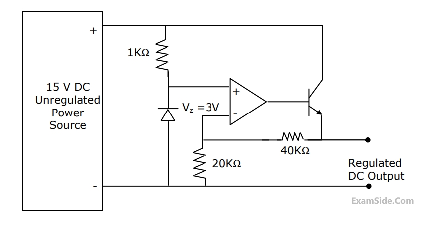
1
The output voltage of the Regulated power supply shown in the figure is
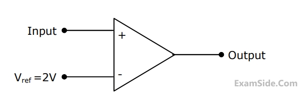
2
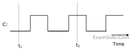
If the input to the ideal comparator shown in figure is sinusoidal signal of 8V
(peak to peak) without any DC component, then the output of the comparator
has a duty cycle of
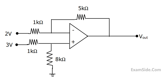
3
If the Op-Amp in the figure is ideal, the output voltage V
out will equal to
4
An amplifier without feedback has a voltage gain of 50, input Resistance of 1 k$$\Omega $$ and output Resistance of 2.5 k$$\Omega $$ . The input Resistance of the current-shunt negative feedback factor of 0.2 is
5
If the differential voltage gain and the common mode voltage gain of a differential Amplifier are 48 dB and 2 dB respectively, then it's common mode Rejection Ratio is
6
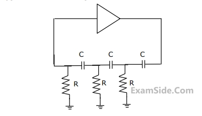
The circuit shown in figure is best described as a
7
The oscillator circuit shown in the figure has an ideal inverting Amplifier. It's frequency of Oscillation (in Hz) is
8
The action of a JFET in its equivalent circuit can be best represented as a
9
An ideal sawtooth voltage waveform of a frequency 500 Hz and Amplitude 3 V is generated by charging a capacitor of 2 $$\mu F$$ in every cycle the charging requires
10
Generally, the gain of a transistor Amplifier falls at high frequency due to the
11
Three identical amplifiers with each one having a voltage gain of 50, input
Resistance of 1 KΩ and output resistance of 250Ω, are cascaded. The open circuit
voltage gain of the combined Amplifier is
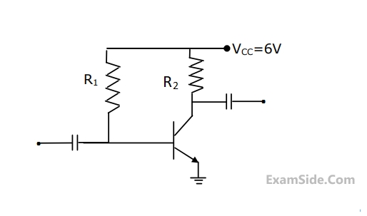
12
In the amplifier circuit shown in the figure, the values of R
1 and R
2 are such that the transistor is operating at V
CE = 3V and I
C = 1.5 mA when its $$\beta $$ is 150. For a transistor with $$\beta $$ of 200, the operating point (V
CE, I
C) is
13
A sinusoidal signal with peak-to-peak amplitude of 1.536V is quantized into 128 levels using a mid-rise uniform quantizer. The quantization-noise power is
14
If Eb, the energy per bit of a binary digital signal, is 10-5 watt-sec and the one-sided power spectral density of the white noise, N0 = 10-6 W/Hz, then the output SNR of the matched filter is
15
A signal is sampled at 8 KHz and is quantized using 8-bit uniform quantizer. Assuming $$SN{R_q}$$ for a sinusoidal signal, the correct statement for PCM signal with a bit rate of R is
16
If S represents the carrier synchronization at the receiver and $$\rho $$ represents the bandwidth efficiency, then the correct statement for the coherent binary PSK is
17
The input to a linear delta modulator having a step size $$\Delta $$ = 0.628 is a sine wave with frequency fm and peak amplitude Em. If the sampling frequency fs = 40 KHz. the combination of the sine-wave frequency and the amplitude, where slope overload will take place is
18
Let $$m\left(t\right)\;=\cos\left[\left(4\mathrm\pi\times10^3\right)t\right]$$ be the message signal and
$$c\left(t\right)\;=5\cos\left[2\mathrm\pi\times10^6t\right]$$ be the carrier.
c(t) and m(t) are used to generate an FM signal. If the peak frequency deviation
of the generated FM signal is three times the transmission bandwidth of the AM
singal, then the coefficient of the term $$\cos\left[2\mathrm\pi\left(1008\times10^3\right)t\right]$$ in the FM signal (in
terms of the Bessel coefficients) is
19
Let $$m\left(t\right)\;=\cos\left[\left(4\mathrm\pi\times10^3\right)t\right]$$ be the message signal and
$$c\left(t\right)\;=5\cos\left[2\mathrm\pi\times10^6t\right]$$ be the carrier.
c(t) and m(t) are used to generate an AM signal. The modulation index of the
generated AM signal is 0.5. Then the quantity $$\frac{Total\;sideband\;power}{Carrier\;power}$$ is
20
A DSB-SC signal is to be generated with a carrier frequency fc = 1MHz using a
nonlinear device with the input-output characteristic $$v_0=a_0v_i\;+\;a_1v_i^3$$.where a0 and a1 are constants. The output of the nonlinear device can be filtered
by an appropriate band-pass filter. Let $$v_0=A_c'\;\cos\left(2{\mathrm{πf}}_\mathrm c'\mathrm t\right)\;+\;m\left(t\right)$$ where m(t) is the message signal. Then the value of
$$f_c'$$ (in MHz) is
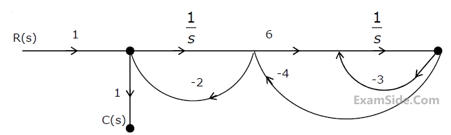
21
The signal flow graph of a system is shown in figure. The transfer function $$\frac{C(s)}{R(s)}$$ of the system is
22
Let x(t) be the input to a linear, time-invariant system. The required output is
4x(t-2). The transfer function of the system should be
23
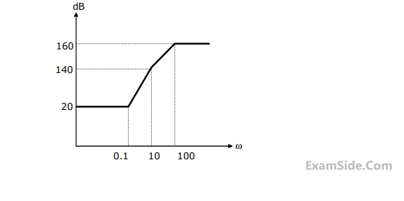
The approximate Bode magnitude plot of a minimum-phase system is shown in
figure. The transfer function of the system is
24
The zero, input response of a system given by the state space equation
$$$\left[ {{{\mathop {{x_1}}\limits^ \bullet } \over {\mathop {{x_2}}\limits^ \bullet }}} \right] = \left[ {\matrix{
1 & 0 \cr
1 & 1 \cr
} } \right]\left[ {\matrix{
{{x_1}} \cr
{{x_2}} \cr
} } \right]and\left[ {\matrix{
{{x_1}} & {\left( 0 \right)} \cr
{{x_2}} & {\left( 0 \right)} \cr
} } \right] = \left[ {\matrix{
1 \cr
0 \cr
} } \right]is$$$
25
A PD controller is used to compensate a system. Compared to the
uncompensated system, the compensated system has
26
The gain margin and the phase margin of a feedback system with
G(s)H(s)=$${s \over {{{\left( {s + 100} \right)}^3}}}$$ are
27
The gain margin for the system with open-loop transfer function G(s)H(s)=$${{2(1 + s)} \over {{s^2}}}$$ is
28
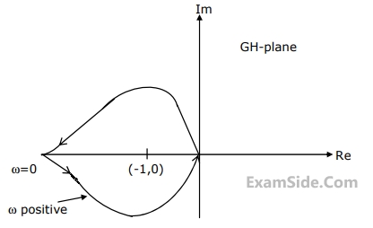
Figure shows the Nyquist plot of the open-loop transfer function G(s)H(s) of a
system. If G(s)H(s) has one right hand pole, the closed loop system is
29
The root locus of the system $$$G\left(s\right)H\left(s\right)=\frac K{s\left(s+2\right)\left(s+3\right)}$$$ has the break-away point
located at
30
The open-loop transfer function of a unity feedback system is $$$G\left(s\right)=\frac k{s\left(s^2+s+2\right)\left(s+3\right)}$$$ the range of 'k' for which the system is stable
31
A second-order system has the transfer function $$\frac{C\left(s\right)}{R\left(s\right)}=\frac4{s^2+4s+4}$$. With r(t) as the unit-step function, the response c(t) of the system is represented
by
32
A 0 to 6 counter consist of 3 flip-flops and a combination circuit of 2 input gate(s). The combination circuit consists of
33
The circuit shown in figure is a 4-bit DAC
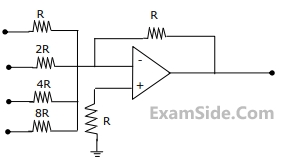
The input bits 0 and 1 are represented by 0 and 5 V respectively. The OP- AMP is ideal, but all the resistances and the 5V inputs have a tolerance of ±10%.
The specification (rounded to the nearest multiple of 5%) for the tolerance of the DAC is
34
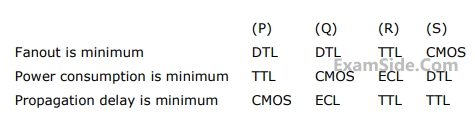
The DTL, TTL, ECL and CMOS families of digital ICs are compared in the following 4 columns
35
The output of the 74 series of TTL gates is taken from a BJT in
36
A 4 bit ripple counter and a 4 bit synchronous counter are made using flip-flops having a propagation delay of 10 ns each. If the worst case delay in the ripple counter and the synchronous counter be R and S respectively, then
37
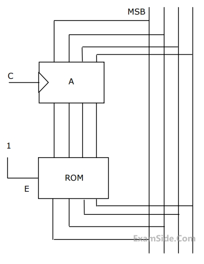
In the circuit shown in Figure, A is a parallel in, parallel-out 4-bit register, which loads at the rising edge of the clock C. The input lines are connected to a 4-bit bus, W. Its output acts as the input to a 16×4 ROM whose output is floating when
the enable input E is 0. A partial table of the contents of the ROM is as follows

The clock to the register is shown, and the data on the W bus at time t$$_1$$ is 0110. The data on the bus at time t$$_2$$ is
38
With out any additional circuitry, an 8:1 MUX can be used to obtain
39
The circuit shown in figure has 4 boxes each described by inputs P, Q, R and outputs Y, Z with
Y = $$\,P \oplus \,Q\, \oplus \,R$$
z= $$RQ + \overline P R\, + Q\,\overline P $$
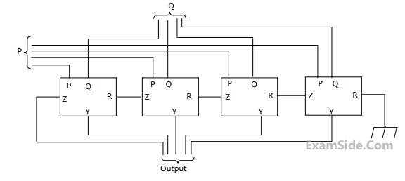
The circuit acts as a
40
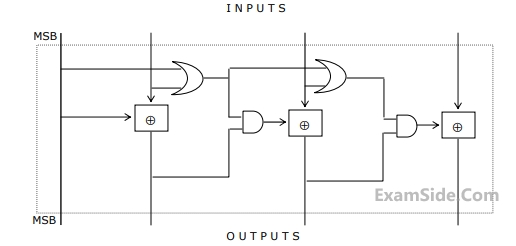
The circuit shown in figure converts
41
If the functions W, X, Y and Z are as follows
W= R+$$\overline P Q + \overline R $$ S
X = $$X = PQ\overline R \,\overline S + \overline P \,\overline Q \,\overline R \,\overline S + P\overline Q \,\overline R \,\overline S $$
Y = $$RS + \overline {OR + P\overline Q + \overline {PQ} } $$
Z = $$R + S + \overline {PQ + \overline {PQR} + P\overline {QS} } $$
42
The number of distinct Boolean expressions of 4 variables is
43
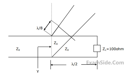
A short-circuited stub is shunt connected to a transmission line as shown in Fig. If $${Z_0} = 50\,\,\Omega $$, the admittance Y seen at the junction of the stub and the transmission line is
44
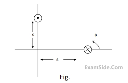
Two identical antennas are placed in the $$\theta = \pi /2$$
plane as shown in figure. The
elements have equal amplitude excitation with 180° polarity difference, operating
at wavelength λ. The correct value of the magnitude of the far zone resultant
electric field strength normalized with that of a single element, both computed for $$\phi = 0$$ is
45
A rectangular metal wave guide filled with a dielectric material of relative permittivity $${\varepsilon _r} = \,4$$ has the inside dimensions $$3.0\,cm\,\, \times \,\,1.2\,cm$$. The cut-off frequency for the dominant mode is
46
If the electric field intensity associated with a uniform plane electromagnetic wave traveling in a perfect dielectric medium is given by
$$E\left( {z,\,t} \right) = \,10\,\cos \left( {2\pi \times {{10}^7}\,\,t - 0.1\,\,\pi z} \right)\,$$ volt/m, the velocity of the traveling wave is
47
Medium $$1$$ has the electrical permittivity $${\varepsilon _1} = 1.5\,\,{\varepsilon _0}\,\,\,F/m$$ and occupies the region to left of $$x = 0$$ plane. Medium $$2$$ has the electrical permittivity $${\varepsilon _2} = 2.5\,\,{\varepsilon _0}\,\,\,F/m$$ and occupies the region to the right of $$x = 0$$ plane. If $${E_1}$$ in medium $$1$$ is $${E_1} = \left( {2\,{u_x} - 3\,{u_y} + 1\,{u_z}} \right)$$ volt/m, then $${E_2}$$ in medium $$2$$ is
48
A uniform plane wave traveling in air is incident on the plane boundary between air and another dielectric medium with $${\varepsilon _r} = 4$$. The reflection coefficient for the normal incidence, is
49
The depth of penetration of electromagnetic wave in a medium having conductivity $$\sigma $$ at a frequency of 1 KHz is 25 cm. The depth of penetration at a frequency of 4 KHz will be
50
If the electric field intensity is given by $$\mathrm E=\left(\mathrm x{\widehat{\mathrm u}}_\mathrm x\;+\mathrm y{\widehat{\mathrm u}}_\mathrm y+\mathrm z{\widehat{\mathrm u}}_\mathrm z\right)\;\mathrm{volt}/\mathrm m$$, the potential
difference between X(2,0,0) and Y(1,2,3) is
51
The unit of $$\nabla\times\mathrm H$$ is
52
n-type silicon is obtained by doping silicon with
53
At 300 K, for a diode current of 1 mA, a certain germanium diode requires a
forward bias of 0.1435 V. Where as a certain silicon diode requires a forward bias
of 0.718 V. Under the conditions stated above, the closest approximation of the
ratio of reverse saturation current in germanium diode to that in silicon diode is
54
An n-type silicon bar 0.1 cm long and $$100\;\mu m^2$$ in cross-sectional area has a majority
carrier concentration of $$5\times10^{20}/m^3$$ and the carrier mobility is $$0.13\;\;m^2/v-s\;$$ at
300oK. if the charge of an electron is 1.6×10⁻¹⁹ coulomb, then the resistance of the
bar is
55
The electron concentration in a sample of uniformly doped n-type silicon at 300oK varies linearly from $$10^{17}/cm^3$$ at x = 0 to $$6\times10^{16}/cm^3$$ at x = 2 $$\mu m$$. Assume a situation that electrons are supplied to keep this concentration gradient constant with time.If electronic charge is $$1.6\times10^{-19}\;coulomb$$ and the diffusion constant $$D_n=3\;cm^2/s$$, the current density in the silicon, if no electric field is present is
56
Choose proper substitutes for X and Y to make the following statement correct
Tunnel diode and Avalanche photodiode are operated in X bias and Y bias
respectively.
57
If P is Passivation, Q is n-well implant, R is metallization and S is source/drain
diffusion, then the order in which they are carried out in a standard n-well CMOS
fabrication process, is
58
When the gate-to-source voltage (VGS) of a MOSFET with threshold voltage of
400 mV, working in saturation is 900 mV, the drain current is observed to be 1
mA. Neglecting the channel width modulation effect and assuming that the
MOSFET is operating at saturation, the drain current for an applied VGS of 1400
mV is
59
For an n-channel enhancement type MOSFET, if the source is connected at a
higher potential than that of the bulk (i.e. VSB > 0), the threshold voltage VT of
the MOSFET will
60
The laplace transform of $$i(t)$$ is given by
$$I\left( s \right) = {2 \over {s\left( {1 + s} \right)}}$$ As $$t \to \infty ,$$ the value of $$i(t)$$ tends to __________.
61
In an 8085 microprocessor, the instruction CMP B has been executed while the
content of the accumulator is less than that of register B. As a result
62
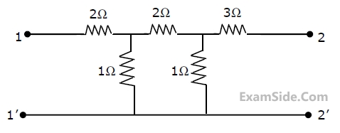
Find the Y-parameters (short ciruit admittance parameters) for the network shown in figure.

63
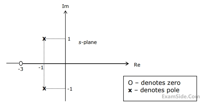
The driving-point impedance Z(s) of a network has the pole-zero locations as shown in figure. If Z(0) = 3, then Z(s) is
64
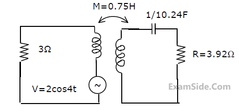
An input voltage $$v(t)$$ $$ = 10\sqrt 2 \,\,\cos \,\,\left( {t + {{10}^0}} \right) + 10\sqrt 5 \,\,\cos \left( {2t + {{10}^0}} \right)\,\,V$$ is applied to a series combination of resistance $$L = 1H$$. the resulting steady - state current $$i(t)$$ in ampere is
65
The minimum number of equations required to analyze the circuit shown in Fig.

66
The impedance parameters Z
11 and Z
12 of the two-port network in figure are
67
The current flowing through the resistance R in the circuit in figure has the form
P cos 4t, where P is
68
A series RLC circuit has a resonance frequency of 1 kHz and a quality factor Q =
100. If each R, L and C is doubled from its original value, the new Q of the circuit
is
69
The circuit is given in figure.Assume that the
switch S is in position 1 for a long time and thrown to position 2 at t = 0.
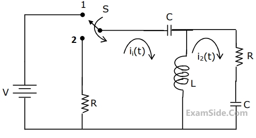
I1(s) and I2(s) are the Laplace transforms of i1(t) and i2(t) respectively. The
equations for the loop currents I1(s) and I2(s) for the circuit shown in figure, after the switch is brought from position 1 to position 2 at t = 0, are
70
The circuit is given in figure.Assume that the
switch S is in position 1 for a long time and thrown to position 2 at t = 0.
At t = 0+, the current i1 is
71
A source of angular frequency 1rad/sec has source impedance consisting of $$1\Omega$$ resistance in series with 1H inductance. The load that will obtain maximum power transfer is
72
Twelve 1Ω resistances are used as edges to form a cube. The resistance between
two diagonally opposite corners of the cube is
73
A sequence $$x\left( n \right)$$ with the $$z$$-transform $$X\left( z \right)$$ $$ = {z^4} + {z^2} - 2z + 2 - 3{z^{ - 4}}$$ is applied as an input to a linear, time-invariant system with the impulse response $$h\left( n \right) = 2\delta \left( {n - 3} \right)$$
where $$\matrix{
{\delta \left( n \right) = 1,} & {n = 0} \cr
{0,} & {otherwise} \cr
} $$
The output at $$n = 4$$ is
74
Let x(t) be the input to a linear, time-invariant system. The required output is 4x(t - 2). The transfer function of the system should be
75
The Laplace transform of i(t) tends to
$$I\left( s \right)\,\, = \,{2 \over {s\left( {1 + s} \right)}}$$
As $$t \to \infty $$ , the value of i(t) tends to
76
Let P be linearity, Q be time-invariance, R be causality and S be stability.
A discrete time system has the input-output relationship,
$$y\left( n \right) = \left\{ {\matrix{
{x\left( n \right),} & {n \ge 1} \cr
{0,} & {n = 0} \cr
{x\left( {n + 1} \right),} & {n \le - 1} \cr
} } \right.$$
Where $$x\left( n \right)\,$$ is the input and $$y\left( n \right)\,$$ is the output. The above system has the properties
77
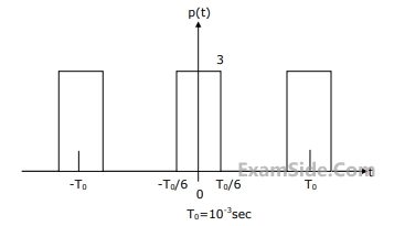
Let x(t) = $$\,2\cos (800\pi t) + \cos (1400\pi t)$$. x(t) is sampled with the rectangular pulse train shown in figure. The only spectral components (in KHz) present in the sampled signal in the frequency range 2.5 kHz to 3.5 kHz are
78
The system under consideration is an RC low -pass filter (RC-LPF) with R = 1.0 $$k\Omega $$ and C = 1.0 $$\mu F$$.
Let $${t_g}$$ (f) be the group delay function of the given RC-LPF and $${f_2}$$ = 100 Hz. Then $${t_g}$$$${(f_2)}$$ in ms, is
79
The system under consideration is an RC low -pass filter (RC-LPF) with R = 1.0 $$k\Omega $$ and C = 1.0 $$\mu F$$.
Let H(t) denote the frequency response of the RC-LPF. Let $${f_1}$$ be the highest frequency such that $$0 \le \left| f \right| \le {f_1},{{\left| {H({f_1})} \right|} \over {H(0)}} \ge 0.95$$. Then $${f_1}$$ (in Hz) is