1
An Op-Amp has an offset voltage of 1mV and is ideal in all other respects. If this OP-Amp is used in the circuit shown in fig. The O/P voltage will be (Select the nearest value).

2
Consider the circuit shown in Fig. The circuit uses an ideal operational amplifier. Assuming that the impedances at noodes A and B do not load the preceeding bridge circuit, calculate the output voltage V
o.
when $${R_a}\, = \,{R_b}\, = \,{R_c}\,{R_d}\,$$ ohms.
when $${R_a}\, = \,{R_b}\, = {R_c}\, = 100$$ ohms and $${R_{d\,}}\, = \,120$$ ohms.

3
The circuit of fig. uses an ideal OP_Amp for small positive values of V
in, the circuit works as

4
If the transistors in fig. has high value of β and a v
BE of 0.65, the
current I flowing through the 2 kilo ohms resistance will be ______.

5
An n-channel JFET has a pinch-off voltage of Vp = -5V. VDS(max) = 20V and gm = 2mA/V. The minimum 'ON' resistance is achieved in the JFET for
6
The JFET in the circuit shown in fig. has an I
DSS = 10mA and V
p = -5V. The value of the resistance R
s for a drain current I
DS = 6.4mA is (select the Nearest value).

7
Assume that the operational amplifier in figure is deal the current I through the
IK ohm resistor is

8
The bit stream 01001 is differentially encoded using 'Delay and Ex OR' scheme for DPSK transmission. Assuming the reference bit as a '1' and assigning phases of '0' and '$$\,\pi $$' for 1's and 0's respectively, in the encoded sequence, the transmitted phase sequence becomes
9
Coherent demodulation of FSK signal can be effected using
10
Source encoding in a data communication system is done in order to
11
For a random variable 'X' following the probability density function, p (x), shown in figure, the mean and the variance are, respectively.

12
The maximum power efficiency of an AM modulator is
13
Block diagram model of a position control system is shown in figure.

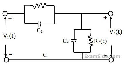
(a) In absence of derivative feedback (K
t=0) , determine damping ratio of the
system for amplifier gain K
A=5. Also find the steady state error to unit
ramp input.
(b) Find suitable values of the parameters K
A and K
t so that damping ratio of the
system is increased to 0.7 without affecting the steady state error as
obtained in part (a).
14
Given a unity feedback system with open loop transfer function,
$$$G\left(s\right)=\frac K{s\left(s+1\right)\left(s+2\right)}$$$
The root locus plot of the system is of the form.
15
Bode plot of a stable system is shown in fig. The transfer function of the system is

16
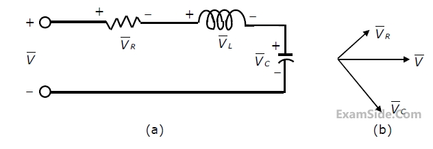
A unity feedback system has open-loop transfer function
$$G(s) = {1 \over {s\left( {2s + 1} \right)\left( {s + 1} \right)}}$$
Sketch Nyquist plot for the system and there from obtain the gain margin and the
phase margin.
17
A process with open-loop model
$$G(s) = {{K{e^{ - s{\tau _d}}}} \over {\tau s + 1}},$$ is controlled by a PID controller. For this process
18
A linear time-invariant system is described by the state variable model
$$$\left[ {\matrix{
{{{\mathop x\limits^ \bullet }_1}} \cr
{{{\mathop x\limits^ \bullet }_2}} \cr
} } \right] = \left[ {\matrix{
{ - 1} & 0 \cr
0 & { - 2} \cr
} } \right]\left[ {\matrix{
{{x_1}} \cr
{{x_2}} \cr
} } \right] + \left[ {\matrix{
0 \cr
1 \cr
} } \right]u.$$$
$$$Y = \left[ {\matrix{
1 & 2 \cr
} } \right]\left[ {\matrix{
{{x_1}} \cr
{{x_2}} \cr
} } \right]$$$
19
The logic realized by the circuit shown in figure is

20
A combinational circuit has three inputs A, B and C and an output F. F is true only for the following input combinations?
A is false and B is true
A is false and C is true
A, B and C are all false
A, B and C are all true.
(a)Write the truth table for F. use the convention, true = 1 and false = 0.
(b)Write the simplified expression for F as a Sum of Products.
(c) Write the simplified expression for F as a product of Sums.
(d) Draw a logic circuit implementation of F using the minimum number of 2
input NAND gates only.
21
The initial contents of the 4-bit serial-in-parallel-out, right-shift, Shift Register shown in figure is 0110. After three clock pulses are applied, the contents of the Shift Register will be

22
Choose the correct satatement(s) from the following:
23
The figure shows the circuit of a gate in the Resistor Transistor Logic (RTL) family. The circuit represents a

24
A new clocked "X-Y" flip-flop is defined with two inputs, X and Y in addition to the clock input. The flip-flop functions as follows:
If XY=00, the flip-flop changes stage with each clock pulse.
If XY=01, the flip-flop state Q becomes 1 with the next clock pulse.
If XY=10, the flip-flop state Q becomes 0 with the next clock pulse.
If XY=11, no change of state occurs with the clock pulse.
(a) Write the Truth table for the X-Y flip flop
(b) Write the Excitation table for the X-Y flip flop
(c) It is desired to convert a J-K flip flop into the X-Y flip flop by adding some external gates, if necessary. Draw a circuit to show how you will implement the X-Y flip-flop using a J-K flip-flop.
25
A transmission line whose characteristic impedance is a pure resistance
26
A uniform plane wave traveling in free space along the +$$z$$ direction and having its electric field along the$$ x$$-direction, is normally incident on a thick brass sheet, infinite in extent (along the $$x$$-and $$y$$-directions). The electric field intensity of the wave is given by
$$${E_x} = 1225\,\cos \,\left( {5.89 \times {{10}^{10}}t - \beta z} \right)\,\,\,\,V/m$$$.
Calculate the power per square metre that causes heating of the brass sheet, taking $${ \in _r} = 1,\,\,\,{\mu _r} = 1$$ and
$$\sigma = 1.649 \times {10^7}\,\,\,\,\,$$ mhos/metre for brass.
27
Two dissimilar antennas having their maximum directivities equal
28
The beam width-between-first-null of a uniform linear array of N equally-spaced (element spacing = d) equally-excited antennas is determined by
29
Elements of a linear array of three equally spaced (element spacing $$0.5\lambda $$ ) vertical mast radiators are excited as given in Fig. For the horizontal plane radiation pattern of the array determine the direction of the major lobe (main lobe or principal lobe) and calculate its half-power-beam-width in degrees.

30
A semiconductor is irradiated with light such that carriers are uniformly
generated throughout its volume. The semiconductor is n-type with $$N_D=10^{19}/cm^3$$. If the excess electron concentration in the steady state id $$\triangle n=10^{15}/cm^3$$ and if $$\tau_p=10\;\mu\;sec$$ [minority carrier life time] the generation rate due to
irradiation
31
The 6 V Zener diode shown in figure has zero Zener resistance and a knee current
of 5 mA. The minimum value of R, so that the voltage across it does not fall below
6 V is:

32
In a transistor having finite B, the forward bias across the base emitter junction
is kept constant and the reverse bias across the collector base junction is
increased. Neglecting the leakage across the collector base junction and the
depletion region generating current, the base current will __________.
(increase/decrease/remain constant).
33
An n-channel JFET has a pinch-off voltage VP = -5 V, VDS(max) = 20 V and gm = 2 mA/V. The minimum ‘ON’ resistance is achieved in the JEFT for
34
The following program is run on 8085 microprocessor:

At the completion of execution of the program, the program Counter of the 8085 contains ________ and the Stack Pointer contains ________.
35
In an 8085 microprocessor system with memory mapped I/O,
36
The two-port Darlington impedance booster of figure uses identical transistors $$({h_{ie}} = 1\,k,\,\,{h_{fe}} = \,100,\,\,{h_{re}} = \,\,{h_{oe}} = \,0$$. Calculate the z-parameters of the network. (Use relavant approximations)

37
For the compensated attenuator of figure, the impulse response under the
condition $$R_1C_1\;=\;R_2C_2$$ is:
38
For the series R-L-C circuit of figure(a), the partial phasor diagram at a certain
frequency is shown in figure (b).The operating frequency of the circuit is:
39
For a 2-port network to be reciprocal
40
Relative to a given fixed tree of a network
41
Of the four networks, N1,N2, N3 and N4 of figure, the networks having identical
driving point functions are

42
A low pass signal x(t) has a spectrum given by $$X(f) = \left\{ {\matrix{
{1 - \left| f \right|/2000,} & {for\,\,\left| f \right|\, \le \,2000\,Hz} \cr
{0,} & {elsewhere} \cr
} } \right.$$
Assuming that x(t) is ideally sampled at a sampling frequency of 3 kHz, sketch
(i) x(f), and
(ii) the spectrum of the sampled signal for $${\,\left| f \right|\, \le \,\,3\,kHz}$$.
43
If G(f) represents the Fourier transform of a signal g (t) which is real and odd symmetric in time, then
44
A linear discrete - time system has the characteristic equation, $${z^3} - 0.81\,\,z = 0.$$ The system
45
Which of the following signals is/are periodic?