Digital Circuits
Number System and Code Convertions
Marks 1Marks 2
Sequential Circuits
Marks 1Marks 2Marks 5Marks 8
Semiconductor Memories
Marks 1Marks 2
Logic Families
Marks 1Marks 2Marks 8
Analog to Digital and Digital to Analog Converters
Marks 1Marks 2
1
GATE ECE 1998
MCQ (Single Correct Answer)
+1
-0.3
The noise margin of a TTL gate is about
A
0.2V
B
0.4V
C
0.6V
D
0.8V
2
GATE ECE 1998
MCQ (Single Correct Answer)
+1
-0.3
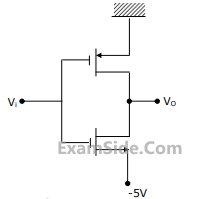
The threshold voltage for each transistor in Fig.2.5, is 2V. For this circuit to work as an inverter, Vi must take the values GATE ECE 1998 Digital Circuits - Logic Families Question 18 English
A
-5 V and 0 V
B
-5 V and 5 V
C
-0 V and 3 V
D
3 V and 5 V
3
GATE ECE 1997
MCQ (Single Correct Answer)
+1
-0.3
For the NMOS logic gate shown in figure, the logic function implemented is GATE ECE 1997 Digital Circuits - Logic Families Question 20 English
A
$$\overline {ABCDE} $$
B
$$(AB + \overline C ).(\overline {D + E} )$$
C
$$\overline {A.(B + C) + D.E} $$
D
$$(\overline {A + B} ).C + \overline D .\overline E $$
4
GATE ECE 1997
MCQ (Single Correct Answer)
+1
-0.3
The gate delay of an NMOS inverter is dominated by charge time rather than discharge time because
A
the driver transistor has a larger threshold voltage than the load transistor.
B
the driver transistor has larger leakage currents compared to the load transistor.
C
the load transistor has a smaller W/L ratio compared to the driver transistor
D
none of the above
GATE ECE Subjects
Signals and Systems
Network Theory
Control Systems
Digital Circuits
General Aptitude
Electronic Devices and VLSI
Analog Circuits
Engineering Mathematics
Microprocessors
Communications
Electromagnetics