Digital Circuits
1
GATE ECE 2007
MCQ (Single Correct Answer)
+2
-0.6
The circuit diagram of a standard TTL NOT gate is shown in the figure. When $${V_i}$$= 2.5V, the modes of operation of the transistors will be:

2
GATE ECE 2003
MCQ (Single Correct Answer)
+2
-0.6
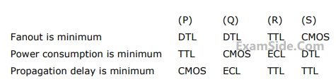
The DTL, TTL, ECL and CMOS families of digital ICs are compared in the following 4 columns
3
GATE ECE 1994
True or False
+2
-0
In the output stage of a standard TTL, we have a diode between the emitter of the pull up transistor and the collector of the pull-down transistor. The purpose of this diode is to isolate the output node from the power supply $${V_{cc}}$$.
4
GATE ECE 1987
MCQ (Single Correct Answer)
+2
-0.6
Given that for a logic family,
$${V_{OH}}$$ is the minimum output high-level voltage
$${V_{OL}}$$ is the minimum output low-level voltage
$${V_{IH}}$$ is the minimum output high-level voltage and
$${V_{IL}}$$ is the minimum output low-level voltage.
The correct relationship is:
Questions Asked from Marks 2
GATE ECE Subjects
Signals and Systems
Network Theory
Control Systems
Digital Circuits
General Aptitude
Electronic Devices and VLSI
Analog Circuits
Engineering Mathematics
Microprocessors
Communications
Electromagnetics