1
GATE ECE 2014 Set 4
MCQ (Single Correct Answer)
+2
-0.6
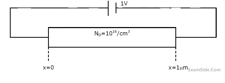
An N-type semiconductor having uniform doping is biased as shown in the figure.

If EC is the lowest energy level of the conduction band, EV is the highest energy level of the valance band and EF is the Fermi level, which one of the following represents the energy band diagram for the biased N-type semiconductor?
A

B

C

D

2
GATE ECE 2014 Set 2
Numerical
+2
-0
Assume electronic charge q = 1.6×10⁻¹⁹ C, kT/q = 25 mV and electron mobility μn = 1000
cm2/V-s. If the concentration gradient of electrons injected into a P-type silicon sample is
1×10²¹/cm4, the magnitude of electron diffusion current density (in A/cm2) is _________.
Your input ____
3
GATE ECE 2010
MCQ (Single Correct Answer)
+2
-0.6
The silicon sample with unit cross-sectional area shown below is in thermal
equilibrium. The following information is given: T=300K, electronic charge=1.6x10-
19C, thermal voltage=26mV and electron mobility = 1350cm2/V-s
The magnitude of the electron drift current density at x=0.5 μm is
4
GATE ECE 2010
MCQ (Single Correct Answer)
+2
-0.6
The silicon sample with unit cross-sectional area shown below is in thermal
equilibrium. The following information is given: T=300K, electronic charge=1.6x10-
19C, thermal voltage=26mV and electron mobility = 1350cm2/V-s
The magnitude of the electric field at x=0.5 μm is
Questions Asked from Marks 2
GATE ECE Subjects
Signals and Systems
Network Theory
Control Systems
Digital Circuits
General Aptitude
Electronic Devices and VLSI
Analog Circuits
Engineering Mathematics
Microprocessors
Communications
Electromagnetics