Analog Circuits
1
GATE ECE 1999
Subjective
+5
-0
A bipolar junction transistor amplifier circuit is shown in the figure. Assume that the current source Ibias is ideal, and the transistor has very large$$\beta ,\,\,{r_{b\,\,}} = \,\,0,$$ and the $${r_0}\, \to \,\infty $$.
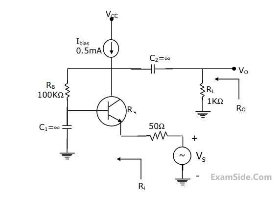
Determine the ac small-signal mid-band and voltage gain $$\left( {{V_o}/{V_s}} \right),$$ input resistance (R1, and output resistance (R0) of the circuit. Assume $${V_{T\,\,}} = \,\,26\,mV.$$
2
GATE ECE 1998
Subjective
+5
-0
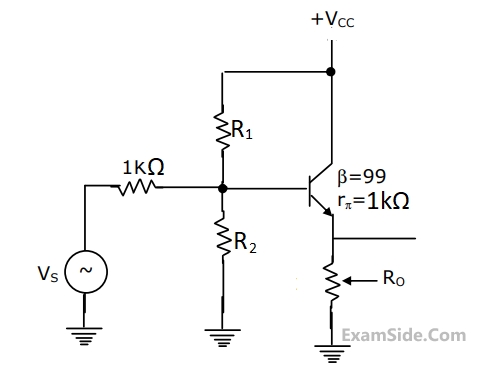
In the circuit of fig. Determine the resistance Ro seen by the output terminals, ignore the effects of R1 and R2.
3
GATE ECE 1997
Subjective
+5
-0
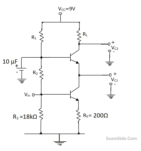
The transistor in the circuit shown in the figure. is so biased (dc biasing N/W is not shown) that the dc collector current IC = 1mA. Supply is VCC = 5V.

The N/W components have following values, RC = 2$$k\Omega $$,
RS = $$1.4k\Omega $$,
RE = $$100\Omega $$.
The transistor has specifications, $$\beta \,\, = \,\,100$$
and base spreading resistance $${r_{bb\,}}^1\, = \,100\Omega $$
Evaluate input resistance Ri for two cases. At a frequency of 10 kHz
(a)CE, the bypass capacitor across RE is 25 $$\mu F$$
(b)The bypass capacitor CE is removed leaving RE unbypassed.
4
GATE ECE 1997
Subjective
+5
-0
In the cascade amplifier circuit shown below, determine the values of R1, R2 and RL. Such that the quiescent current through the transistors is 1mA and the collector voltage Vc1 = 3V, and Vc2 = 6V. Tke VBE = 0.7V, Transistor $$\beta $$ to be hifgh and base currents to be negligible.
Questions Asked from Marks 5
GATE ECE Subjects
Signals and Systems
Network Theory
Control Systems
Digital Circuits
General Aptitude
Electronic Devices and VLSI
Analog Circuits
Engineering Mathematics
Microprocessors
Communications
Electromagnetics