For a MOS capacitor, $$\mathrm{V_{fb}}$$ and $$\mathrm{V_{t}}$$ are the flat-band voltage and the threshold voltage, respectively. The variation of the depletion width ($$\mathrm{W_{dep}}$$) for varying gate voltage ($$\mathrm{V_{g}}$$) is best represented by
 The logic implemented by the circuit is


P: As channel length reduces, OFF-state current increases.
Q:As channel length reduces, output resistance increases.
R: As channel length reduces, threshold voltage remains constant.
S: As channel length reduces, ON current increases.


S1: The threshold voltage (VT) of a MOS capacitor decreases with increase in gate
oxide thickness
S2: The threshold voltage (VT) of a MOS capacitor decreases with increase in
substrate doping concentration.
Consider a MOS capacitor made with p-type silicon. It has an oxide thickness of 100 nm, a fixed positive oxide charge of $10^{-8}$ C/cm2 at the oxide-silicon interface, and a metal work function of 4.6 eV. Assume that the relative permittivity of the oxide is 4 and the absolute permittivity of free space is $8.85 × 10^{-14}$ F/cm. If the flatband voltage is 0 V, the work function of the p-type silicon (in eV, rounded off to two decimal places) is ______.
In the circuit below, the voltage V$$_{\mathrm{L}}$$ is _____________ V (rounded off to two decimal places).


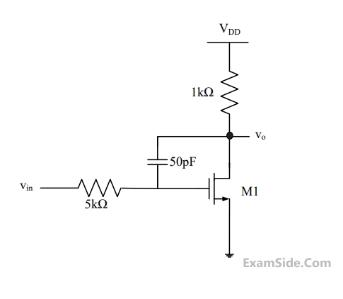
gm = 0.5$$\mu {\rm A}/V$$ for VDS = 50 m V and VGS = 2V,
gd = $$8\mu {\rm A}/V$$ for VGS = 2 V and VDS = 0 V,
Where gm =$${{\partial {{\rm I}_D}} \over {\partial {V_{GS}}}}\,\,and\,\,{g_d}\,\, = \,{{\partial {{\rm I}_D}} \over {\partial {V_{DS}}}}$$
The threshold voltage (in volts) of the transistor is


K=$${1 \over 2}\mu {C_{OX}}\left( {{W \over L}} \right) = 0.1mA/{V^2}$$ . The value of ID (in mA) is _______


kN = $${\mu _n}{C_{ox}^{'}}$$ (W/L)= 40$$\mu {\rm A}/{V^2},$$ threshold voltage VTN=1V, and neglect body effect and channel length modulation effects)


The source-body junction capacitance is approximately
The gate-source overlap capacitance is approximately

Estimate the output voltage V0 for VG =1.5 V. [Hints: Use the appropriate current-voltage equation for each MOSFET, based on the answer]
For small increase in VG beyond 1 V, which of the following gives the correct description of the region of operation of each MOSFET?
 The current Ix is related to Ibias as
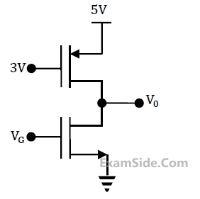
Kn = Kp = μnCOX$$\frac{W_n}{L_n}$$ = μpCOX$$\frac{W_P}{L_P}$$= 40 μA/V2 and their threshold voltages are VT = 1 V, the current I is:

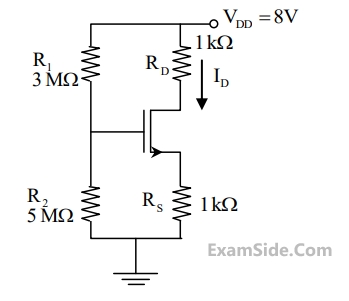
(i) VGS = 0 at ID = 12 mA and
(ii) VGS = - 6 Volts at ID = 0
Which of the following Q-points will give the highest trans-conductance gain for small signals?