Combinational Circuits
Practice Questions
Marks 1
1

A full adder and an XOR gate are used to design a digital circuit with inputs $X, Y$, and $Z$, and output $F$, as shown below. The input $Z$ is connected to the carry-in input of the full adder.

If the input $Z$ is set to logic ' 1 ', then the circuit functions as __________ with $X$ and $Y$ as inputs.

GATE ECE 2025 Digital Circuits - Combinational Circuits Question 1 English
GATE ECE 2025
2

In the circuit shown below, P and Q are the inputs. The logical function realized by the circuit shown below is

GATE ECE 2023 Digital Circuits - Combinational Circuits Question 4 English

GATE ECE 2023
3

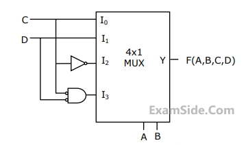
Consider the 2-bit multiplexer (MUX) shown in the figure. For OUTPUT to be the XOR of C and D, the values for A0, A1, A2 and A3 are ___________.

GATE ECE 2022 Digital Circuits - Combinational Circuits Question 5 English

GATE ECE 2022
4
Consider the circuit shown in the figure. GATE ECE 2017 Set 2 Digital Circuits - Combinational Circuits Question 38 English The Boolean expression F implemented by the circuit is
GATE ECE 2017 Set 2
5
A 4:1 multiplexer is to be used for generating the output carry of a full adder. A and B are the bits to be added while 𝐢in is the input carry and 𝐢out is the output carry. A and B are to be used as the select bits with A being the more significant select bit. GATE ECE 2016 Set 2 Digital Circuits - Combinational Circuits Question 39 English Which one of the following statements correctly describes the choice of signals to be connected to the inputs $${I_0}$$, $${I_1}$$, $${I_2 }$$ and $${I_3}$$ so that the output is C$$_{out}$$?
GATE ECE 2016 Set 2
6
In a half-subtractor circuit with X and Y as inputs, the Borrow (M) and Difference (N = X - Y) are given by
GATE ECE 2014 Set 2
7
The output Y of a 2-bit comparator is logic 1 whenever the 2-bit input A is greater than the 2-bit input B. The number of combinations for which the output is logic 1, is
GATE ECE 2012
8
The logic function implemented by the circuit below is (ground implies a logic "0" GATE ECE 2011 Digital Circuits - Combinational Circuits Question 42 English
GATE ECE 2011
9
The Boolean function f implemented in the figure using two input multiplexers is GATE ECE 2005 Digital Circuits - Combinational Circuits Question 10 English
GATE ECE 2005
10
With out any additional circuitry, an 8:1 MUX can be used to obtain
GATE ECE 2003
11
A 2-bit binary multiplier can be implemented using
GATE ECE 1997
12
The output of the circuit shown in figure is equal to GATE ECE 1995 Digital Circuits - Combinational Circuits Question 13 English
GATE ECE 1995
13
The logic realized by the circuit shown in figure is GATE ECE 1992 Digital Circuits - Combinational Circuits Question 14 English
GATE ECE 1992
14
The minimum function that can detect a "divisible by 3" 8421 BCD code digit (representation is D8 D4 D2 D1) is given by:
GATE ECE 1990
Marks 2
1

A 4-bit priority encoder has inputs $D_3, D_2, D_1,$ and $D_0$ in descending order of priority. The two-bit output $AB$ is generated as 00, 01, 10, and 11 corresponding to inputs $D_3, D_2, D_1,$ and $D_0$, respectively. The Boolean expression of the output bit $B$ is _______.

GATE ECE 2024
2

The propagation delay of the 2 x 1 MUX shown in the circuit is 10 ns. Consider the propagation delay of the inverter as 0 ns.

GATE ECE 2024 Digital Circuits - Combinational Circuits Question 2 English

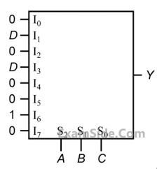
If S is set to 1 then the output Y is _______.

GATE ECE 2024
3
A four-variable Boolean function is realized using 4 $$ \times $$ 1 multiplexers as shown in the figure. GATE ECE 2018 Digital Circuits - Combinational Circuits Question 6 English
The minimized expression for F(U, V, W, X) is
GATE ECE 2018
4
Figure I shows a 4-bits ripple carry adder realized using full adders and Figure II shows the circuit of a full-adder (FA). The propagation delay of the XOR, AND and OR gates in Figure II are 20 ns, 15 ns and 10 ns respectively. Assume all the inputs to the 4-bit adder are initially reset to 0. GATE ECE 2017 Set 2 Digital Circuits - Combinational Circuits Question 19 English 1 GATE ECE 2017 Set 2 Digital Circuits - Combinational Circuits Question 19 English 2 
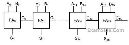
At t=0, the inputs to the 4-bit adder are changed to $${X_3}$$$${X_2}$$$${X_1}$$$${X_0}$$ =1100, $${Y_3}$$$${Y_2}$$$${Y_1}$$$${Y_0}$$ = 0100 and $${Z_0}$$=1. The output of the ripple carry adder will be stable at t (in ns) = ____
GATE ECE 2017 Set 2
5
A programmable logic array (PLA) is shown in the figure. GATE ECE 2017 Set 2 Digital Circuits - Combinational Circuits Question 20 English The Boolean function F implemented is
GATE ECE 2017 Set 2
6
For the circuit shown in the figure, the delays of NOR gates, multiplexers and inverters are 2 ns, 1.5 ns and 1 ns, respectively. If all the inputs P, Q, R, S and T are applied at the same time instant, the maximum propagation delay (in ns) of the circuit is ___________. GATE ECE 2016 Set 3 Digital Circuits - Combinational Circuits Question 21 English
GATE ECE 2016 Set 3
7
Identify the circuit below. GATE ECE 2016 Set 1 Digital Circuits - Combinational Circuits Question 23 English
GATE ECE 2016 Set 1
8
The functionality implemented by the circuit below is GATE ECE 2016 Set 1 Digital Circuits - Combinational Circuits Question 22 English
GATE ECE 2016 Set 1
9
A 1-to-8 demultiplexer with data input D$$_{in}$$ , address inputs S$$_{0}$$, S$$_{1}$$, S$$_{2}$$ (with S$$_{0}$$ as the LSB) and $${\overline Y _0}$$ to $${\overline Y _7}$$ as the eight demultiplexed outputs, is to be designed using two 2-to-4 decoders (with enable input $$\overline E $$ and address inputs A$$_{0}$$ and A$$_{1}$$) as shown in the figure. $${D_{in}}$$, S$$_{0}$$, S$$_{1}$$and S$$_{2}$$ are to be connected to P, Q, R and S, but not necessarily in this order. The respective input connections to P, Q, R, and S terminals should be GATE ECE 2015 Set 2 Digital Circuits - Combinational Circuits Question 24 English
GATE ECE 2015 Set 2
10
An 8-to-1 multiplexer is used to implement a logical function Y as shown in the figure. The output Y is given by GATE ECE 2014 Set 4 Digital Circuits - Combinational Circuits Question 26 English
GATE ECE 2014 Set 4
11
A 16-bit ripple carry adder is realized using 16 identical full adders (FA) as shown in the figure. The carry-propagation delay of each FA is 12 ns and the sum-propagation delay of each FA is 15 ns. The worst case delay (in ns) of this 16-bit adder will be_______________. GATE ECE 2014 Set 4 Digital Circuits - Combinational Circuits Question 25 English
GATE ECE 2014 Set 4
12
If X and Y are inputs and the Difference (D = X – Y) and the Borrow (B) are the outputs, which one of the following diagrams implements a half-subtractor?
GATE ECE 2014 Set 3
13
In the circuit shown, π‘Šπ‘Š and π‘Œπ‘Œ are MSBs of the control inputs. The output 𝐹𝐹 is given by GATE ECE 2014 Set 3 Digital Circuits - Combinational Circuits Question 28 English
GATE ECE 2014 Set 3
14
The Boolean function realized by the logic circuit shown is GATE ECE 2010 Digital Circuits - Combinational Circuits Question 29 English
GATE ECE 2010
15
What are the minimum number of 2-to 1 multiplexers required to generate a 2-input AND gate and a 2-input EX-OR gate?
GATE ECE 2009
16
For the circuit shown in the following figure $${I_0}$$ - $${I_3}$$ are inputs to the 4:1 multiplexer R(MSB) and S are control bits. tHE OUTPUT Zcan be represented by GATE ECE 2008 Digital Circuits - Combinational Circuits Question 31 English
GATE ECE 2008
17
In the following circuit, X is given by GATE ECE 2007 Digital Circuits - Combinational Circuits Question 32 English
GATE ECE 2007
18
The minimum number of 2 to 1 multiplexers required to realize a 4 to 1 mutliplexer is
GATE ECE 2004
19
The circuit shown in figure has 4 boxes each described by inputs P, Q, R and outputs Y, Z with
Y = $$\,P \oplus \,Q\, \oplus \,R$$
z= $$RQ + \overline P R\, + Q\,\overline P $$ GATE ECE 2003 Digital Circuits - Combinational Circuits Question 34 English 
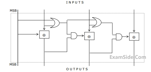
The circuit acts as a
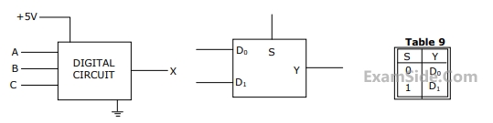
GATE ECE 2003
20
The circuit shown in figure converts GATE ECE 2003 Digital Circuits - Combinational Circuits Question 35 English
GATE ECE 2003
21
In the TTL circuit in Figure 2.11, $${S_0}$$ to $${S_0}$$ are select lines and $${X_7}$$ and $${X_0}$$are input lines. $${S_0}$$ and $${X_0}$$ are LSB'. The output Y is GATE ECE 2001 Digital Circuits - Combinational Circuits Question 36 English
GATE ECE 2001
22
For a binary half-sub-tractor having two inputs A and B, the correct set of logical expressions for the outputs D (=A minus B) and X (=borrow) are
GATE ECE 1999
Marks 10
1
A ROM is to be used to implement the Boolean functions given below:
$${F_1}$$$$(A,\,B,\,C,\,D) = ABCD + \bar A\,\overline B \,\bar C\,\bar D$$
$${F_2}(A,\,B,\,C,\,D) = (A + B)(\bar A\, + \overline B + C)$$
$${F_3}(A,\,B,\,C,\,D) = \sum {13,15 + \sum {3,5} } $$

(a) What is the minimum size of the ROM required?

(b) Determine the data in each location of the ROM.

GATE ECE 1995
2
A Boolean function, F , given as sum of product (SOP) terms as F= $$\sum {} $$m(3,4,5,6) with A,B, and C as inputs. The function, F, can be expreeed on the Karnaugh's map shown below.

(1) What will be the minimized SOP expression for F?
(2) Implement this function on an 8 : 1 MUX.

GATE ECE 1994
3
Signals A,B,C,D and $$\overline D $$ are available. Using a single 8 - to - 1 multiplexer and no other gate, implement the Boolean function.

$$f(A,B,C,D) = B.C + A.B.\bar D + \bar A.\bar C.\bar D$$
GATE ECE 1993
4
A chemical reactor has three sensors indicating the following conditions:-
(1) Pressure (P) is low or high'
(2) Temperature (T) is low or high' and
(3) Liquid level (L) is low or high.

its has two controls - Heater (H) which is either on or off and inlet value (V) which is open or close. The controls are operated as per Table.

(a) Using the convertion High =1, Low = 0, On=1, Off=0, Open=1 and Closed=0, draw the Karnaugh maps for H and V.

(b) Obtain the minimal product of sums expressions for H and V.

(c) Realize the logic for H and V using two 4-input multiplexers with T and L as control inputs. Used T as MSB. GATE ECE 1989 Digital Circuits - Combinational Circuits Question 8 English

GATE ECE 1989