Analog to Digital and Digital to Analog Converters
Practice Questions
Marks 1
1
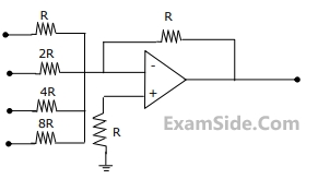
A 4-bit weighted-resistor DAC with inputs $b_3, b_2, b_1$, and $b_0$ (MSB to LSB) is designed using an ideal opamp, as shown below. The switches are closed when the corresponding input bits are logic ' 1 ' and open otherwise. When the input $b_3 b_2 b_1 b_0$ changes from 1110 to 1101, the magnitude of the change in the output voltage $V_O$ (in mV , rounded off to the nearest integer) is ____________. GATE ECE 2025 Digital Circuits - Analog to Digital and Digital to Analog Converters Question 1 English
GATE ECE 2025
2

The signal-to-noise ratio (SNR) of an ADC with a full-scale sinusoidal input is given to be 61.96 dB. The resolution of the ADC is __________ bits (rounded off to the nearest integer).

GATE ECE 2023
3
Consider a four bit D to A converter. The analog value corresponding to digital signals of values 0000 and 0001 are 0 V and 0.0625 V respectively. The analog value (in Volts ) corresponding to the digitals signal 1111 is ______________.
GATE ECE 2015 Set 1
4
The number of comparators required in a 3-bit comparator type ADC is
GATE ECE 2002
5
The number of comparators in 4-bit flash ADC is
GATE ECE 2000
6
The resolution of a 4-bit counting ADC is 0.5 Volts. For an analog input of 6.6 Volts, the digital output of the ADC will be
GATE ECE 1999
7
The advantage of using a dual slope ADC in a digital voltmeter is that
GATE ECE 1998
8
For an ADC, match the following : if
List 1
A. Flash converter
B. Dual slope converter
C. Successive approximation Converter

List 2
1. requires a conversion time of the order of a few seconds
2. requires a digital- to- analog converter
3. minimizes the effect of power supply interference.
4. requires a very complex hardware.
5. It is a tracking A/D converter.
GATE ECE 1998
9
A 12-bit ADC is operating with a 1$$\mu $$ sec clock period and the total conversion time is seen to be 14 $$\mu $$ sec. The ADC must br of the
GATE ECE 1996
10
Match the List-1 (type of 8-bit ADC) with List-2(Minimum conversion time in clock cycles)

List - 1


A. Successive approximation
B. Dual-slope
C. Parallel Comparator

List - 2


1) 1
2) 8
3) 16
4) 256
5) 512
GATE ECE 1994
11
Which of the resistance networks of figure can be used as 3 bit R-2R ladder DAC. Assume $${V_0}$$ corresponds to LSB. GATE ECE 1990 Digital Circuits - Analog to Digital and Digital to Analog Converters Question 12 English 1 GATE ECE 1990 Digital Circuits - Analog to Digital and Digital to Analog Converters Question 12 English 2 GATE ECE 1990 Digital Circuits - Analog to Digital and Digital to Analog Converters Question 12 English 3
GATE ECE 1990
Marks 2
1
A 10-bit analog-to-digital converter (ADC) has a sampling frequency of 1 MHz and a full scale voltage of 3.3 V . For an input sinusoidal signal with frequency 500 kHz , the maximum SNR (in dB, rounded off to two decimal places) and the data rate (in Mbps) at the output of the ADC are _________ , respectively.
GATE ECE 2025
2

A full scale sinusoidal signal is applied to a 10-bit ADC. The fundamental signal component in the ADC output has a normalized power of 1 W, and the total noise and distortion normalized power is 10 $\mu$W. The effective number of bits (rounded off to the nearest integer) of the ADC is _______.

GATE ECE 2024
3

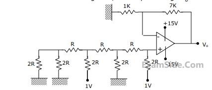
Consider the circuit shown with an ideal OPAMP. The output voltage V0 is __________ V (rounded off to two decimal places).

GATE ECE 2022 Digital Circuits - Analog to Digital and Digital to Analog Converters Question 5 English

GATE ECE 2022
4
In an N bit flash ADC, the analog voltage is fed simultaneously to 2N− 1 comparators. The output of the comparators is then encoded to a binary format using digital circuits. Assume that the analog voltage source Vin(whose output is being converted to digital format) has a source resistance of 75 Ω as shown in the circuit diagram below and the input capacitance of each comparator is 8 pF. The input must settle to an accuracy of 1/2 LSB even for a full scale input change for properconversion. Assume that the time taken by the thermometer to binary encoder is negligible. GATE ECE 2016 Set 2 Digital Circuits - Analog to Digital and Digital to Analog Converters Question 11 English If the flash ADC has 8 bit resolution, which one of the following alternatives is closest to the maximum sampling rate?
GATE ECE 2016 Set 2
5
In the following circuit, the comparator output is logic “I” if V1 > V2 and is logic “0” otherwise. The D/A conversion is done as per the relation $$${V_{DAC}} = \sum\limits_{n = 0}^3 {{2^{n - 1}}{b_n}\,\,} Volts,$$$ where b3(MSB), b2, b1 and b0 (LSB) are the counter outputs.

The counter starts from the clear state.

GATE ECE 2008 Digital Circuits - Analog to Digital and Digital to Analog Converters Question 6 English

The magnitude of the error between VDAC and Vin at steady state in volts is

GATE ECE 2008
6
In the following circuit, the comparator output is logic “I” if V1 > V2 and is logic “0” otherwise. The D/A conversion is done as per the relation $$${V_{DAC}} = \sum\limits_{n = 0}^3 {{2^{n - 1}}{b_n}\,\,} Volts,$$$ where b3(MSB), b2, b1 and b0 (LSB) are the counter outputs.

The counter starts from the clear state.

GATE ECE 2008 Digital Circuits - Analog to Digital and Digital to Analog Converters Question 7 English

The stable reading of the LED display is

GATE ECE 2008
7
In the digital-to-Analog converter circuit shown in the figure below,
$${V_{R\,}}\, = \,10V$$ and $$R\, = \,10k\Omega $$ GATE ECE 2007 Digital Circuits - Analog to Digital and Digital to Analog Converters Question 9 English

The current i is

GATE ECE 2007
8
In the digital-to-Analog converter circuit shown in the figure below,
$${V_{R\,}}\, = \,10V$$ and $$R\, = \,10k\Omega $$ GATE ECE 2007 Digital Circuits - Analog to Digital and Digital to Analog Converters Question 8 English

The voltage V0 is

GATE ECE 2007
9
A 4-bit D/A converter is connected to a free-running 3-bit UP counter, as shown in the following figure. Which of the following waveforms will be observed at V0=? GATE ECE 2006 Digital Circuits - Analog to Digital and Digital to Analog Converters Question 10 English

In the figure shown above, the ground has been shown by the symbol $$\nabla $$
GATE ECE 2006
10
The circuit shown in figure is a 4-bit DAC GATE ECE 2003 Digital Circuits - Analog to Digital and Digital to Analog Converters Question 14 English The input bits 0 and 1 are represented by 0 and 5 V respectively. The OP- AMP is ideal, but all the resistances and the 5V inputs have a tolerance of ±10%.
The specification (rounded to the nearest multiple of 5%) for the tolerance of the DAC is
GATE ECE 2003
11
For the 4 bit DAC shown in Figure, the output voltage $${V_0}$$ is GATE ECE 2000 Digital Circuits - Analog to Digital and Digital to Analog Converters Question 15 English
GATE ECE 2000